

Table of Contents
Introduction
Material innovations in the field of organic semiconductors (P3HT, PEDOT:PSS), MoS₂ and graphene are core areas of modern research and development. Thin-film technologies open up a wide range of possible applications, from flexible electronics to energy-efficient sensors. Precise measurement methods are essential for targeted process control, component optimization and basic material characterization. This is where the Thin Film Analyzer (TFA) as a universal platform offers methodical strengths that are decisive for innovations in the R&D environment.
Methodical advantages of the Thin Film Analyzer
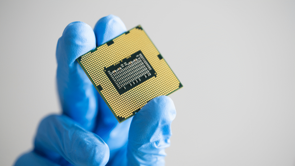
The Thin Film Analyzer (TFA) is not just a classic measuring device, but a flexible, chip-based measuring platform for the comprehensive characterization of the physical properties of thin films. This platform allows the simultaneous measurement of several thermal and electrical parameters and thus offers a holistic understanding of the material behavior.
The central measured variables include thermal conductivitywhich is measured with high precision using the established 3-omega method method – specially adapted to the requirements of thin layers. In addition, the electrical conductivity and electrical resistance can be measured using the Van der Pauw configuration can be precisely determined. The spectrum is supplemented by the measurement of the Seebeck coefficient to record thermoelectric properties and optional Hall add-on modules to determine the Hall constant and carrier mobility (1, 2).
The TFA also offers exceptional technical flexibility. It enables the precise investigation of layers in the thickness range between 5 nm and 25 µm. Even complex effects such as surface interactions, grain boundary scattering or quantization can be specifically recorded in real material systems. The platform is universally compatible with a large number of modern deposition processes, including PVD, CVDALD, spin coating and inkjet printing.
The measuring range for thermal conductivity extends from 0.05 to 200 W/m∙K, for electrical conductivity from 0.05 to 1∙10⁶ S/cm. The temperature can be regulated over a wide range from -160 °C to +280 °C – both in an ultra-high vacuum and under a controlled atmosphere (1, 2).
Advantages for the research and development process
Direct correlation of structure-property relationships
Changes in the layer structure or chemical composition can be immediately compared with electrical and thermal properties. This is essential for organic semiconductors such as P3HT and PEDOT:PSS or 2D materials such as MoS₂ and graphene, as their functionality strongly depends on layer morphology, interfaces and processing. The TFA method enables the precise determination of crucial parameters on ultrathin films and shows particular sensitivity to surface and interface effects (3, 4).
Validation and optimization of deposition processes
- Rapid quantification of changes due to various process parameters such as substrate temperature or layer thickness
- Systematic process screening for PEDOT:PSS/MoS₂ composites and similar material systems
- Direct linking of different processing conditions (temperature steps, solvent, layer thickness) with resulting layer properties
- Massive acceleration of iteration cycles through simultaneous measurements of several physical properties on one sample chip
- Efficient elucidation of the relationship between molecular arrangement (edge-on/face-on morphology in P3HT) and resulting conductivity (4, 5)
Industry proximity and reproducibility
- Established and standardizable methods (Van-der-Pauw, 3-Omega) ensure high comparability
- Seamless transfer from laboratory scale to production-related process environments
- Decisive advantage for upscaling and technology transfer to industrial applications
- Good comparability between different laboratories, processed batches and subsequent industrial applications (2)
Specific applications for modern material systems
Modern material systems such as organic semiconductors – including P3HT and PEDOT:PSS in particular – enable precise characterization of special electronic and thermal transport mechanisms. A direct correlation can be established between targeted manipulation of the film structure, for example through exposure to light during coating, and the resulting electrical power. The close relationship between electrical power and the morphology of the film – for example an edge-on or face-on orientation – is also immediately comprehensible. These deep insights into the relationships between structure and properties open up new possibilities for the targeted development of more efficient materials and components. It is particularly advantageous that only small sample quantities are required for the analysis – just a few micrograms of material are sufficient (6).
2D materials such as MoS₂ and graphene also offer a wide range of potential applications. The focus here is on the control and evaluation of deposition conditions, crystallinity and electrical contacts. The targeted analysis of transport channels, interfacial effects and the influences of various growth processes can provide crucial insights. In addition, the characterization of unique transport phenomena with regard to charge carrier density and mobility in layered composites enables a deeper understanding of these materials. The combination of in-plane and out-of-plane characterization opens up innovative approaches for the development of new component concepts. Precise knowledge of the interface and transport specifics is particularly important for vertical and hybrid component architectures (7, 8).
Differences to other thin film analysis methods
Multifunctional integration vs. individual measurements
The TFA combines several established measuring principles on one measuring chip: thermal conductivity (3-omega method), electrical transport properties (Van der Pauw method), Seebeck coefficient and optionally charge carrier mobility, density and Hall coefficient. This makes it possible to measure several key physical parameters of a thin film with only one setup and a single sample preparation on the same sample with identical geometry, thus minimizing sources of error due to sample differences (1, 2).
Consistent measurement conditions
In contrast to classic individual analyses with separate measurement setups, TFA delivers consistent, comparable values under identical environmental conditions. All measurements are carried out in the same direction (in the film, in-plane), which avoids systematic differences due to measurement set-up, temperature control or contacting type, as can occur with classic methods (standalone 3-omega, separate four-point measurements) (1, 2).
Simplified sample handling
- Chip-based technology with pre-structured measurement carriers simplifies complex contacting considerably
- Significantly lower sample requirement compared to classic FTIR or ATR spectroscopy methods
- Fast measurements with largely automated evaluation
- No complex preparation required as with standalone test benches (TGA, DSC, Hall test benches)
- Universal applicability for different material classes: Semiconductors, metals, organic materials, ceramics (1, 2)
Practical relevance for research and development
Increased efficiency in everyday laboratory work
- Multimodal measurements: Thermal, electrical and Seebeck parameters on a single sample without complex conversion
- Enormous acceleration of research cycles through simultaneous parameter acquisition
- Automated, temperature- and atmosphere-controlled measurements for high reproducibility
- Continuity and reliability in the R&D process, especially in early development phases with limited material (1, 2)
Material-specific advantages
- Analytically leading methods for special semiconductors such as PEDOT:PSS/CuO/MoS₂ structures
- Optimal characterization of ultra-thin organic functional layers
- Sensitivity to fine structures and interfaces in organic semiconductors and 2D materials
- Direct visualization of the effect of process and treatment parameters on material parameters (4, 5)
Technology transfer and scaling
- State-of-the-art requirements in the laboratory environment: from temperature control and vacuum conditions to simple automation and data integration
- Standardized measurement principles support comparability across different laboratories
- Facilitated transfer of research results into industrial development
- Direct transfer of research data to applications using established, industry-compatible methods (2)
Conclusion
The Thin Film Analyzer (TFA) functions as a universal “toolbox” for R&D laboratories and offers a methodologically solid foundation for the targeted development, analysis and optimization of novel material systems. The platform is specially tailored to the requirements of a research-oriented laboratory environment and shortens iteration cycles, increases the significance of the measurement data and offers the flexibility required for successful R&D in the field of modern thin-film materials.
Research on organic semiconductors and 2D materials (MoS₂, graphene) benefits from the unique combination of versatility, speed and precision of the TFA methodology. The method supports data-driven, iterative design of advanced functional materials and devices from targeted layer development to rapid evaluation of new concepts for accelerated and data-driven material innovation in modern research laboratories.
List of sources
- Linseis – Megalab: Linseis – Thin Film Analysis (TFA) – Megalab
https://megalab.gr/en/product/linseis-thin-film-analysis-tfa/ - TFA L59 – LINSEIS: TFA L59 Thin-Film Analyzer – LINSEIS
https://www.linseis.com/en/instruments/electrical-property/thin-film-thin-film-analysis/tfa-l59/ - Charge Transport Across Au-P3HT-Graphene van der Waals Heterostructures
https://pubs.acs.org/doi/10.1021/acsami.2c13148 - Solution-Processed PEDOT:PSS/MoS₂ Nanocomposites as Efficient Electrodes
https://www.mdpi.com/2079-4991/9/9/1328 - Organic-inorganic p-type PEDOT:PSS/CuO/MoS₂ photocathode
https://www.sciencedirect.com/science/article/pii/S2214993723001847 - Morphology of Organic Semiconductors Probed by GIWAXS – Xenocs
https://www.xenocs.com/how-does-visible-light-impact-the-morphology-of-organic-semiconductors/ - Synthesis and Characterization of 2D Materials: Graphene and Molybdenum Disulfide
https://bearworks.missouristate.edu/theses/1601/ - Stretchable Thin-Film Transistors Based on Wrinkled Graphene and MoS₂
https://experts.illinois.edu/en/datasets/stretchable-thin-film-transistors-based-on-wrinkled-graphene-and-
