Physical properties of thin-films are becoming more and more important in industries and applications such as phase-change materials, optical disk media, thermoelectric materials, light emitting diodes (LEDs), fuel cells, phase change memories, flat panel displays, and the semiconductor industry in general.
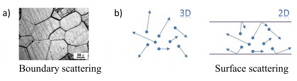
All these industries use single or multi-layer setups in order to give a device a particular function. Since the physical properties of thin films differ significantly from bulk material, it is necessary to obtain their thickness and temperature dependent properties with matching characterization devices. Due to the high aspect ratios and deposition techniques, additional boundary and surface scattering occurs, resulting in reduced transport properties.
As the requirements for the measurement may differ from bulk material, different metrology needs to be used.
The thermal conductivity and electrical conductivity of thin film materials is usually smaller than that of their bulk counterparts, sometimes dramatically so. For example, at room temperature, lambda of a 20 nm Si film or nanowire can be a factor of five smaller [1] than its bulk single-crystalline counterpart. For 100 nm of Au it could be shown, that the transport properties are nearly cut in halve [2]. Generally one can say, that the transport properties are not only temperature but also strongly thickness dependent [3].
Such thermal conductivity reductions generally occur for two basic reasons. First, compared to bulk single crystals, many thin film synthesis technologies result in more impurities, disorder, and grain boundaries, all of which tend to reduce the thermal conductivity. Second, even an atomically perfect thin film is expected to have reduced thermal conductivity due to boundary scattering, phonon leakage, and related interactions. Both basic mechanisms generally affect in-plane and crossplane transport differently, so that the thermal conductivity of thin films is usually anisotropic, even for materials whose bulk forms have an isotropic lambda.
[1] Li, Deyu, et al. “Thermal conductivity of individual silicon nanowires.” Applied Physics Letters 83.14 (2003): 2934-2936.
[2] Linseis, V., Völklein, F., Reith, H., Nielsch, K., and Woias, P. 2018. Thermoelectric properties of Au and Ti nanofilms, characterized with a novel measurement platform. Materials Today: Proceedings, ECT2017 Conference Proceedings.
[3] Linseis, V., Völklein, F., Reith, H., Hühne, R., Schnatmann, L., Nielsch, K., and Woias, P. 2018. Thickness and temperature dependent thermoelectric properties of Bi87Sb13 nanofilms measured with a novel measurement platform. Semiconductor Science and Technology.